ATLANT 3D Nanosystems is a Danish deep-tech startup company with a pioneering vision of democratising and diversifying advanced technologies. We are the first to invent atomic layer 3D printing for rapid prototyping and fabrication of micro and nanodevices with more than 450 different materials. We are a cross European with a vibrant and interdisciplinary R&D and entrepreneurial team. You will get the opportunity to work with groundbreaking technology and top specialists in the field.
DESCRIPTION
ABOUT THE COMPANY AND THE ROLE
ATLANT 3D Nanosystems is committed to developing innovative manufacturing technologies for future smart automated micro and nanofactories. We are continuously looking for deep-tech driven people who are not afraid to dream big and are passionate to solve challenges. You will be in the foundation of a microsystem design group, this position will support the development of our core technology and core industrial applications primarily in the Copenhagen area, Denmark. The goal of the microsystem development group is to investigate, test, and develop new micro and nanofabrication methods and tools.
WANT TO BUILD THE FUTURE OF NANOTECHNOLOGY?
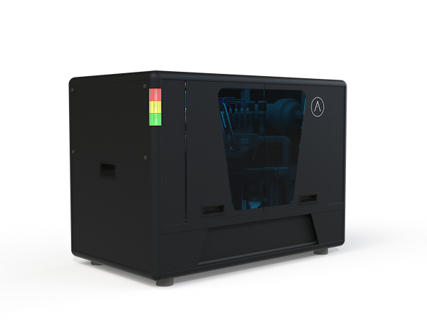
We are a team of rebels, dreamers, and go-getters with a vision to change the World. At ATLANT 3D Nanosystems we are actively developing the next generation of the first-ever atomic layer 3D printer, a foundation system for the factories of the future, with the ultimate goal to enable smart rapid innovation for a better future on Earth or in Space.
ARE YOU A VISIONARY DOER? COME BUILD A PRODUCT OUT OF THIS WORLD WITH US!
You will be working with a vibrant and interdisciplinary R&D and entrepreneurial startup team that grows rapidly and offers the potential for you to grow as a professional and as a person. ATLANT 3D Nanosystems is a Danish deep-tech startup company with a pioneering vision of democratising and diversifying advanced technologies. We are the first to invent atomic layer 3D printing for rapid prototyping and fabrication of micro and nanodevices with more than 450 different materials. We have grown a team with cross European expertise and several locations. Our success is entirely due to our brilliant and passionate team, partners, and experienced advisers. You will get the opportunity to work with groundbreaking technology and top specialists in the field and to grow and develop new and improved micro/nanofabrication technology - leave your footprint in stone.
CANDIDATE PROFILE
We are looking for visionary team members that can foresee the potential of our technology and are ready to execute small and large steps towards a great vision. As a Micro-/Nanotechnology Engineer, you will be responsible for the fabrication of novel microsystems for and with Nanofabricator™ within our laboratory and DTU Nanolab cleanroom facility using a combination of UV photolithography and laser-based micromachining techniques in collaboration with external industrial partners, customers and R&D institutes across Europe. You will be in the foundation of a microsystem R&D group, this position will lead the development of our core technology and core industrial applications primarily in the Copenhagen area, Denmark and intensively collaborate with several industrial and academic partners and customers across EU. This will include leading the design of the microsystems, development of process flows, and conducting micro and nanofabrication, testing microsystems, development and characterization of new processes and applications. You will cooperate with internal and external team members on the same or similar tasks.
ABOUT YOU
- You have a deep tech curious mindset that triggers you to look for unprecedented challenges and solutions
- You have in-depth knowledge in microsystems, primarily microfluidic or sensor microdevices
- You have proved experience in design, development, testing, and analysis of microsystems, printing processes/structures and demonstrate a range of functionalities in selected applications
- You have experience in CAD and simulation of microsystems and microfabrication processes
- You have a can-do positive attitude, ability to multitask, and a self-starter approach
- You find big challenges exciting and enjoy discovering, defining and solving them
- You deliver. You may enjoy thoughtful conversations about problems and perfecting designs, but in the end, you know that what matters is delivering a solution that works every time
- You are a cross-disciplinary team member with a service approach and ready to have the back of your teammate. You are excited to work and communicate with and learn from various teams: micro and nanotechnologies, material science, chemical synthesis hardware, software development, business development teams or customers, and you are eager to develop new R&D and industrial areas
- You are resourceful, flexible and adaptable; open-minded and seeking alternative solutions, no task is too big or too small
- You are curious and eager to learn and participate in the development of a startup company, tolerate startup chaos and take initiative to organize things, learn from and contribute to the company’s business, customer relations, IP, team building, fundraising, and setting team and company culture.
- You embrace the responsibility to plan and execute R&D work
- You have excellent engineering skills and an analytical mindset
- You have experience and willingness to report your results, prepare articles and patent applications
- You have a talent/experience and desire to lead others
- You have excellent English language skills - You are able to travel up to 20% of your work time across Europe
KEY QUALIFICATIONS
- MSc or PhD degree in Micro and Nanofabrication, Physics, Chemistry or related fields
- Extensive cleanroom experience, wet chemistry experience (3+ years)
- Valid training and certifications from EU, preferably Nordic/DTU Nanolab cleanroom facilities
- Proficiency in mask design and mechanical CAD design (3+ years)
- Hands-on experience in UV photolithography processes and equipment (3+ years)
- Experience with DRIE of silicon and thin-film techniques (3+ years)
- Hands-on experience with laser micromachining methods
- Experience with thin-film techniques: ALD, CVD, e-beam and sputter deposition techniques etc.
- Proficiency with microdevice and nanomaterials characterisation: electrical, SEM, AFM, XRD, XPS, Ellipsometry measurements techniques etc. (3+ years)
- Track record of scientific articles, patent, grant applications and willingness to write new ones
- Intensive experience with DoE, data processing, analysis, report preparation skills, preferably with Origin, LaTEX/MS Word, MS PowerPoint etc.
- Excellent analytical and communication skills
- Simulation experience preferably in physics and computational fluid dynamics
- Familiarity with various methods of micro and nanotechnology
AS A PLUS, YOU ALSO HAVE EXPERIENCE IN:
- Fundraising with R&D funds and managing reporting procedure
- Deep tech startup development and startup investments
- Having experience in scientific instruments, vacuum systems, thin-film equipment design, development, and maintenance
- Expertise in one of the following fields, nanoparticles catalysis, biomedical microfluidic devices, photonics, optics, fiber optics, chemical reactors and synthesis, ALD, thin-film technologies etc.
- Programming and general IT skills
- Project management skills, product development lifecycle, and management
- WIllingness to communicate with a customer and lead their projects
- Experience with Solid Works CAD, L-Edit or Clewin mask design software
- Various language skills
SALARY AND TERMS OF EMPLOYMENT
Competitive salary and opportunity to grow. For the best candidates and long term employees, we offer a stocks program. The term of employment is 2 years with the possibility to extend further upon successful implementation of the company strategy.
WORKPLACE
The microfabrication and materials/device characterization will be carried out at DTU Lyngby Campus at DTU Nanolab, providing the infrastructure necessary to conduct the research in this ambitious project. Testing of micronozzle systems with our atomic layer 3D printer will be carried out at two locations - our lab in Lyngby and/or in Friedrich Alexander University in Erlangen in Germany (depending on the process materials requirements).
APPLICATION
Please submit your online application no later than August 1, 2020 (CET).
Applications must be submitted as one PDF file containing all materials to be given consideration.
The file must include:
A letter motivating the application (cover letter)
Curriculum vitae
MSc/PhD diplomas
List of publications/grant applications/patents etc.
List of not academic activities including any business-related, industrial, hobby etc.
Perks and benefits
This job comes with several perks and benefits

Equity package

Skill development

Social gatherings

Free coffee / tea

Free office snacks

Near public transit
Working at
ATLANT 3D